SXM (socket)
SXM (Server PCI Express Module)[1] is a high bandwidth socket solution for connecting Nvidia Compute Accelerators to a system. Each generation of Nvidia Tesla since P100 models, the DGX computer series and the HGX boards come with an SXM socket type that realizes high bandwidth, power delivery and more for the matching GPU daughter cards.[2] Nvidia offers these combinations as an end-user product e.g. in their models of the DGX system series. Current socket generations are SXM for Pascal based GPUs, SXM2 and SXM3 for Volta based GPUs, SXM4 for Ampere based GPUs, and SXM5 for Hopper based GPUs. These sockets are used for specific models of these accelerators, and offer higher performance per card than PCIe equivalents.[2] The DGX-1 system was the first to be equipped with SXM-2 sockets and thus was the first to carry the form factor compatible SXM modules with P100 GPUs and later was unveiled to be capable of allowing upgrading to (or being pre-equipped with) SXM2 modules with V100 GPUs.[3][4]
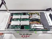
SXM boards are typically built with four or eight GPU slots, although some solutions such as the Nvidia DGX-2 connect multiple boards to deliver high performance. While third party solutions for SXM boards exist, most System Integrators such as Supermicro use prebuilt Nvidia HGX boards, which come in four or eight socket configurations.[5] This solution greatly lowers the cost and difficulty of SXM based GPU servers, and enables compatibility and reliability across all boards of the same generation.
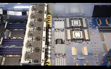
SXM modules on e.g. HGX boards, particularly recent generations, may have NVLink switches to allow faster GPU-to-GPU communication. This as well reduces bottlenecks which would normally be located within CPU and PCIe.[2][6] The GPUs on the daughter cards are just using NVLink as their main communication protocol. For example a Hopper-based H100 SXM5 based GPU can use up to 900 GB/s of bandwidth across 18 NVLink 4 channels, with each contributing a 50 GB/s of bandwidth;[7] This compared to PCIe 5.0, which can handle up to 64 GB/s of bandwidth within a x16 slot.[8] This high bandwidth also means that GPUs can share memory over the NVLink bus, allowing an entire HGX board to present to the host system as a single, massive GPU.[9]
Power delivery is also handled by the SXM socket, negating the need for external power cables such as those needed in PCIe equivalent cards. This, combined with the horizontal mounting allows cooling options of higher efficiency which in turn allows the SXM based GPUs to operate at a much higher TDP. The Hopper-based H100, for example, can draw up to 700W solely from the SXM socket.[10] The lack of cabling also makes assembling and repairing of large systems much easier, and also reduces the possible points of failure.[2]
The early Nvidia Tegra automotive targeted evaluation board, 'Drive PX2', had two MXM (Mobile PCI Express Module) sockets on both sides of the card, this dual MXM design can be considered a predecessor to the Nvidia Tesla implementation of the SXM socket.
Comparison of accelerators used in DGX:[11][12][13]
| Model | Architecture | Socket | FP32 CUDA cores | FP64 cores (excl. tensor) | Mixed INT32/FP32 cores | INT32 cores | Boost clock | Memory clock | Memory bus width | Memory bandwidth | VRAM | Single precision (FP32) | Double precision (FP64) | INT8 (non-tensor) | INT8 dense tensor | INT32 | FP4 dense tensor | FP16 | FP16 dense tensor | bfloat16 dense tensor | TensorFloat-32 (TF32) dense tensor | FP64 dense tensor | Interconnect (NVLink) | GPU | L1 Cache | L2 Cache | TDP | Die size | Transistor count | Process |
|---|---|---|---|---|---|---|---|---|---|---|---|---|---|---|---|---|---|---|---|---|---|---|---|---|---|---|---|---|---|---|
| B200 | Blackwell | N/A | N/A | N/A | N/A | N/A | N/A | 8 Gbit/s HBM3e | 8192-bit | 8 TB/sec | 192 GB HBM3e | N/A | N/A | N/A | 4.5 POPS | N/A | 9 PFLOPS | N/A | 2.25 PFLOPS | 2.25 PFLOPS | 1.2 PFLOPS | 40 TFLOPS | 1.8 TB/sec | GB100 | N/A | N/A | 1000 W | N/A | 208 B | TSMC 4NP |
| B100 | Blackwell | N/A | N/A | N/A | N/A | N/A | N/A | 8 Gbit/s HBM3e | 8192-bit | 8 TB/sec | 192 GB HBM3e | N/A | N/A | N/A | 3.5 POPS | N/A | 7 PFLOPS | N/A | 1.98 PFLOPS | 1.98 PFLOPS | 989 TFLOPS | 30 TFLOPS | 1.8 TB/sec | GB100 | N/A | N/A | 700 W | N/A | 208 B | TSMC 4NP |
| H200 | Hopper | SXM5 | 16896 | 4608 | 16896 | N/A | 1980 MHz | 6.3 Gbit/s HBM3e | 6144-bit | 4.8 TB/sec | 141 GB HBM3e | 67 TFLOPS | 34 TFLOPS | N/A | 1.98 POPS | N/A | N/A | N/A | 990 TFLOPS | 990 TFLOPS | 495 TFLOPS | 67 TFLOPS | 900 GB/sec | GH100 | 25344 KB (192 KB × 132) | 51200 KB | 1000 W | 814 mm2 | 80 B | TSMC 4N |
| H100 | Hopper | SXM5 | 16896 | 4608 | 16896 | N/A | 1980 MHz | 5.2 Gbit/s HBM3 | 5120-bit | 3.35 TB/sec | 80 GB HBM3 | 67 TFLOPS | 34 TFLOPS | N/A | 1.98 POPS | N/A | N/A | N/A | 990 TFLOPS | 990 TFLOPS | 495 TFLOPS | 67 TFLOPS | 900 GB/sec | GH100 | 25344 KB (192 KB × 132) | 51200 KB | 700 W | 814 mm2 | 80 B | TSMC 4N |
| A100 80GB | Ampere | SXM4 | 6912 | 3456 | 6912 | N/A | 1410 MHz | 3.2 Gbit/s HBM2e | 5120-bit | 1.52 TB/sec | 80 GB HBM2e | 19.5 TFLOPS | 9.7 TFLOPS | N/A | 624 TOPS | 19.5 TOPS | N/A | 78 TFLOPS | 312 TFLOPS | 312 TFLOPS | 156 TFLOPS | 19.5 TFLOPS | 600 GB/sec | GA100 | 20736 KB (192 KB × 108) | 40960 KB | 400 W | 826 mm2 | 54.2 B | TSMC N7 |
| A100 40GB | Ampere | SXM4 | 6912 | 3456 | 6912 | N/A | 1410 MHz | 2.4 Gbit/s HBM2 | 5120-bit | 1.52 TB/sec | 40 GB HBM2 | 19.5 TFLOPS | 9.7 TFLOPS | N/A | 624 TOPS | 19.5 TOPS | N/A | 78 TFLOPS | 312 TFLOPS | 312 TFLOPS | 156 TFLOPS | 19.5 TFLOPS | 600 GB/sec | GA100 | 20736 KB (192 KB × 108) | 40960 KB | 400 W | 826 mm2 | 54.2 B | TSMC N7 |
| V100 32GB | Volta | SXM3 | 5120 | 2560 | N/A | 5120 | 1530 MHz | 1.75 Gbit/s HBM2 | 4096-bit | 900 GB/sec | 32 GB HBM2 | 15.7 TFLOPS | 7.8 TFLOPS | 62 TOPS | N/A | 15.7 TOPS | N/A | 31.4 TFLOPS | 125 TFLOPS | N/A | N/A | N/A | 300 GB/sec | GV100 | 10240 KB (128 KB × 80) | 6144 KB | 350 W | 815 mm2 | 21.1 B | TSMC 12FFN |
| V100 16GB | Volta | SXM2 | 5120 | 2560 | N/A | 5120 | 1530 MHz | 1.75 Gbit/s HBM2 | 4096-bit | 900 GB/sec | 16 GB HBM2 | 15.7 TFLOPS | 7.8 TFLOPS | 62 TOPS | N/A | 15.7 TOPS | N/A | 31.4 TFLOPS | 125 TFLOPS | N/A | N/A | N/A | 300 GB/sec | GV100 | 10240 KB (128 KB × 80) | 6144 KB | 300 W | 815 mm2 | 21.1 B | TSMC 12FFN |
| P100 | Pascal | SXM/SXM2 | N/A | 1792 | 3584 | N/A | 1480 MHz | 1.4 Gbit/s HBM2 | 4096-bit | 720 GB/sec | 16 GB HBM2 | 10.6 TFLOPS | 5.3 TFLOPS | N/A | N/A | N/A | N/A | 21.2 TFLOPS | N/A | N/A | N/A | N/A | 160 GB/sec | GP100 | 1344 KB (24 KB × 56) | 4096 KB | 300 W | 610 mm2 | 15.3 B | TSMC 16FF+ |
References
- Michael Brown, W.; et al. (2012). "An Evaluation of Molecular Dynamics Performance on the Hybrid Cray XK6 Supercomputer". Procedia Computer Science. 9: 186–195. doi:10.1016/j.procs.2012.04.020.
- Proud, Matt. "Achieving Maximum Compute Throughput: PCIe vs. SXM2". The Next Platform. Retrieved 2022-03-31.
- Volta architecture whitepaper nvidia.com
- DGX 1 User Guide nvidia.com
- servethehome (2020-05-14). "NVIDIA A100 4x GPU HGX Redstone Platform". ServeTheHome. Retrieved 2022-03-31.
- "NVLink & NVSwitch for Advanced Multi-GPU Communication". NVIDIA.
- "Nvidia's H100 – What It Is, What It Does, and Why It Matters". Data Center Knowledge | News and analysis for the data center industry. 2022-03-23. Retrieved 2022-03-31.
- "Is PCIe 5.0 Worth It? The Benefits of PCIe 5.0 (2022)". www.techreviewer.com. Retrieved 2022-03-31.
- "NVIDIA HGX A100: Powered by A100 GPUs and NVSwitch". NVIDIA. Retrieved 2022-03-31.
- "NVIDIA H100 GPU full details: TSMC N4, HBM3, PCIe 5.0, 700W TDP, more". TweakTown. 2022-03-23. Retrieved 2022-03-31.
- Smith, Ryan (March 22, 2022). "NVIDIA Hopper GPU Architecture and H100 Accelerator Announced: Working Smarter and Harder". AnandTech.
- Smith, Ryan (May 14, 2020). "NVIDIA Ampere Unleashed: NVIDIA Announces New GPU Architecture, A100 GPU, and Accelerator". AnandTech.
- "NVIDIA Tesla V100 tested: near unbelievable GPU power". TweakTown. September 17, 2017.
External links
- Erlangen National High Performance Computing Center page on high performance computing with 4x and 8x A100 per computer node, also showing switch topology dumps.